| (Nanowerk Spotlight) Quantum dots (QDs) are nanoscale crystals of semiconductor material that glow with bright, rich colors when stimulated by an electric current. First discovered in the 1980s, these materials have been the focus of intense research because of their potential to provide significant advantages in a wide variety of optical applications, among them light-emitting diodes (LEDs). Quantum dots are expected to deliver lower cost, higher energy efficiency and greater wavelength control for a wide range of products, including lamps, displays and photovoltaics. | |
| Unfortunately, the toxicity of the elements used for efficient quantum dot based LEDs – CdS, CdSe, and their Pb containing counterparts – is a severe drawback for many applications. Therefore, light-emitting devices which are based on the non-toxic element silicon are extraordinary promising candidates for future QD-lighting applications. | |
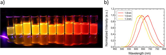
| Researchers in Germany have now demonstrated highly efficient and widely color-tunable silicon light-emitting diodes (SiLEDs). The emission wavelength of the devices can easily be tuned from the deep red (680 nm) down to the orange/yellow (625 nm) spectral region by simply changing the size of the used size-separated silicon nanocrystals. | |
| Reporting their work in the January 15, 2013 online edition of Nano Letters ("Multicolor Silicon Light-Emitting Diodes (SiLEDs)"), a multidisciplinary team at Karlsruhe Institute of Technology, led by Annie K. Powell, Geoffrey A. Ozin and Uli Lemmer, also showed that the size of the silicon nanocrystals has a significant impact on the valence band position of the material. | |
 |
|
| Size-separated silicon nanocrystals (ncSi) and their corresponding PL spectra. (a) Nanoparticles dispersed in toluene showing intense luminescence from the deep red to the yellow spectral region. (b) PL spectra of the three samples used for SiLED fabrication. Excitation: (a) 365 nm LED and (b) 355 nm Nd:YAG laser. (Reprinted with permission from American Chemical Society) | |
| "Compared to other reports on silicon-based LEDs, we show that the emission color can be tuned down to the yellow/orange spectral region whereas existing reports especially focused on NIR-devices," Florian Maier-Flaig, a researcher in Lemmer's group and first author of the paper, tells Nanowerk. "This is the first report of yellow/orange emitting SiLEDs based on size-selected silicon nanocrystals. In addition, size-separation of the particles leads to significantly increased device operation lifetimes." | |
| The team's silicon nanocrystals are capped with allylbenzene and produced by solid-state synthesis. The resulting nanoparticles are colloidally stable in toluene, feature sizes in the range of 1-3 nm, and exhibit photoluminescence quantum yields of up to 43%. | |
| Potential applications are silicon-based light-emitting diodes. Maier-Flaig notes that the use of the particles as down-converting red-emitting “phosphors” for white light generation is also conceivable. The latter are currently fabricated using spectrally broad emitting phosphors which do not feature a strong contribution in the red spectral region being nevertheless crucial for high color rendering indices and generation “warm white” light. | |
| With regard to practical applications, the team cautions that, in order to be compatible with II-VI semiconductor-based QD-LEDs, external quantum efficiency of the devices, quantum efficiency of the nanoparticles itself, as well as long-term stability of the devices should be further improved. | |
 |
|
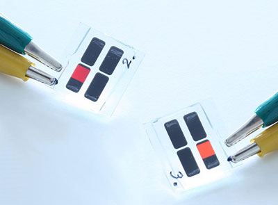
| SiLEDs connected to a 9 V battery in series to an ohmic resistor limiting the voltage to 6 V. The individual photographs are taken at ambient lighting conditions and are not modified with any image processing software. (Reprinted with permission from American Chemical Society. | |
| Referencia: Berger, M. (2013) Silicon LEDS are an alternative to toxic quantum dot LEDs, recuperado el 28 de febrero de 2013, de: http://www.nanowerk.com/spotlight/spotid=28925.php | |
jueves, 28 de febrero de 2013
Silicon LEDS are an alternative to toxic quantum dot LEDs
domingo, 24 de febrero de 2013
Capacitor Nanogate
JEOL Ltd. es uno de los mayores fabricantes japoneses de microscopios electrónicos, quien anunció el desarrollo del capacitor Nanogate, que tiene una densidad de energía de 50 a 75Wh/kg., lo cual es diez veces mayor que la de los actuales capacitores.
Este Capacitor aunque comparte gran aparte de las características de los tradicionales, tiene una mayor densidad de energía que las baterías de níquel-hidrógeno. Tiene ciclos de carga y descarga cortos, una larga vida útil, esta compuesto por carbono y papel aluminio.
Sus aplicaciones en sistemas eléctricos de almacenamiento se estan desarrollando, ya que deben cumplir con las restricciones de tamaño y deben proporcionar la cantidad correcta y la intensidad de la electricidad en la demanda. Los usos que tienen son en vehículos híbridos, vehículos eléctricos, tampones, y dispositivos de almacenamiento de energía solar o eólica. Y se esta viendo su uso en las centrales hidroeléctricas para el bombeo de agua
Mas información: http://www.japanfs.org/en/pages/025429.html
AMOLED (Active Matrix Light Emitting Diode)
AMOLED (Active Matrix Light Emitting Diode) es junto con los OLED (Light Emitting Diode), el futuro y presente de la tecnología para pantallas que se puedever en dispositivos como teléfonos móviles, pantallas de televisión, notebooks.
Los OLEDs son dispositivos ultra delgados y ultra brillantes que no requieren ningún tipo de luz de fondo, sin embargo AMOLED es un tipo específico de tecnología que consiste en un conjunto de cuatro capas: La capa del ánodo, la capa orgánica intermedia, la capa del cátodo y finalmente la que posee toda la circuitería. En la capa del ánodo se sobrepone un conjunto de pixeles OLED que se depositan en una serie de transistores de película fina (TFT), para formar una matriz de pixeles que se iluminan cuando han sido activados eléctricamente, los cuales son controlados por unos interruptores que regulan el flujo de corriente que se dirige a cada uno, lo usual se que la corriente se controle usando dos TFT por pixel, uno se encarga de iniciar y detener la carga del condensador y el otro se encarga de proporcionar el nivel adecuado de tensión al pixel para crear uan tensión constante y evitar los picos de alta tensión, es decir, esta matriz es la encargada de seleccionar que píxeles encender para formar la imagen.
Además gracias a su fabricación con sustratos de plásticos flexibles permite: Reforzados sistemas de protección contra la rotura del dispositivo, un consumo muy bajo en potencia debido a que la matriz requiere mucha menos potencia que una circuitería externa, calidad de imagen mucho mayor, su delgadez y ligereza y una enorme flexibilidad para dicho dispositivos, incluso posibilidad de "enrollarlos" lo que implica facilidad para poderlos transportar o almacenar. Por tanto, todo esto hace que sean mucho más eficaces, lo que provoca que tengan una velocidad más rápida de refresco, ideal para vídeos. Incluso suponen un menor coste que las pantallas LCD.
Empresas como es el caso de Samsung han estado trabajando con esta nueva tecnología ejemplo de ello es el modelo TV AMOLED 17" que sólo tiene 12 mm de grosor que ha desarrollado. Aunque no sólo está trabajando con AMOLED, también está desarrollando una nueva tecnología a partir de esta: "SUPER AMOLED" cuyas principales ventajas son tanto un menor espesor, gracias a la eliminación de las capas superiores táctiles que se incluyen en las pantallas TFT y AMOLED actuales, una mayor calidad de imagen, mayor brillo y contraste, colores más vivos, mejores ángulos de visualización y una respuesta táctil mejorada frente a las pantallas actuales.
Mas información Aqui
lunes, 18 de febrero de 2013
Memoria RaceTrack de IBM
Memoria Racetrack de IBM: la velocidad de la memoria DRAM y capacidad de los discos magnéticos
IBM ha sido capaz de crear un nuevo tipo de memoria no volátil que puede alcanzar las velocidades de la memoria RAM que podemos encontrar en los ordenadores convencionales y la densidad de almacenamiento de los discos duros magnéticos.

La memoria no volátil — que no pierde la información acumulada al no recibir alimentación, y puede usarse por lo tanto como almacenamiento contínuo — desarrollada por la firma americana funciona almacenando bits de información — unos y ceros — en unas pequeñas bandas magnéticas en alambres de nickel y hierro de medidas nanométricas, que pueden ver alterado su orientación magnética al recibir pequeños impulsos eléctricos.
La parte increible es que estos bits se escriben o leen en tan solo 20 o 30 nanosegundos, tiempo infinitamente inferior al de los discos duros más avanzados del mercado actual. Lo que han conseguido los investigadores de IBM con este prototipo es juntar todos los componentes que anteriormente se encontrarían separados de la unidad que contenía los nano-alambres en un solo chip, con tecnología de producción CMOS actual, sin necesidad de adaptarla, lo que haría posible una fabricación en masa instantánea, tan pronto como la tecnología esté lo suficientemente refinada, para lo que quizás todavía falta un tiempo, según la firma.
La característica estrella de la memoria Racetrack es la capacidad potencial de almacenar un gran número de bits en uno solo de esos diminutos alambres, aunque Ravelosona asegura que los materiales utilizados por IBM no tienen las características magnéticas necesarias para ello.
Ese es uno de los obstáculos que IBM deberá superar para traer una tecnología de almacenamiento del futuro a los equipos de "hoy en día", con la capacidad de hacer olvidar a los omnipresentes SSD, y potencialmente, a otras tecnologías igual de prometedoras, como el sistema Moneta del que os hablamos a comienzos del verano. Sin quejas por aquí, cuantas más opciones, mejor para el consumidor.
Fuente: http://gizmologia.com/2011/12/memoria-racetrack-de-ibm-la-velocidad-de-la-memoria-dram-y-capacidad-de-los-discos-magneticos?utm_source=self&utm_medium=nav&utm_campaign=Relacionados
lunes, 4 de febrero de 2013
Organic ferroelectric molecule shows promise for memory chips, sensors .
| At the heart of computing are tiny crystals that transmit and store digital information's ones and zeroes. Today these are hard and brittle materials. But cheap, flexible, nontoxic organic molecules may play a role in the future of hardware. A team led by the University of Washington in Seattle and the Southeast University in China discovered a molecule that shows promise as an organic alternative to today's silicon-based semiconductors. The findings, published this week in the journal Science ("Diisopropylammonium Bromide Is a High-Temperature Molecular Ferroelectric Crystal"), display properties that make it well suited to a wide range of applications in memory, sensing and low-cost energy storage. | |
 http://www.nanowerk.com/news2/newsid=28645.php http://www.nanowerk.com/news2/newsid=28645.php | |
| Electrical response of the newly developed organic crystal. | |
| "This molecule is quite remarkable, with some of the key properties that are comparable with the most popular inorganic crystals," said co-corresponding author Jiangyu Li, a UW associate professor of mechanical engineering. | |
| The carbon-based material could offer even cheaper ways to store digital information; provide a flexible, nontoxic material for medical sensors that would be implanted in the body; and create a less costly, lighter material to harvest energy from natural vibrations. | |
| The new molecule is a ferroelectric, meaning it is positively charged on one side and negatively charged on the other, where the direction can be flipped by applying an electrical field. Synthetic ferroelectrics are now used in some displays, sensors and memory chips. | |
| In the study the authors pitted their molecule against barium titanate, a long-known ferroelectric material that is a standard for performance. Barium titanate is a ceramic crystal and contains titanium; it has largely been replaced in industrial applications by better-performing but lead-containing alternatives. | |
| The new molecule holds its own against the standard-bearer. It has a natural polarization, a measure of how strongly the molecules align to store information, of 23, compared to 26 for barium titanate. To Li's knowledge this is the best organic ferroelectric discovered to date. | |
| A recent study in Nature announced an organic ferroelectric that works at room temperature. By contrast, this molecule retains its properties up to 153 degrees Celsius (307 degrees F), even higher than for barium titanate. | |
| The new molecule also offers a full bag of electric tricks. Its dielectric constant -- a measure of how well it can store energy -- is more than 10 times higher than for other organic ferroelectrics. And it's also a good piezoelectric, meaning it's efficient at converting movement into electricity, which is useful in sensors. | |
| The new molecule is made from bromine, a natural element isolated from sea salt, mixed with carbon, hydrogen and nitrogen (its full name is diisopropylammonium bromide). Researchers dissolved the elements in water and evaporated the liquid to grow the crystal. Because the molecule contains carbon, it is organic, and pivoting chemical bonds allow it to flex. | |
| The molecule would not replace current inorganic materials, Li said, but it could be used in applications where cost, ease of manufacturing, weight, flexibility and toxicity are important. | |
| Li is working on a number of projects relating to ferroelectricity. Last year he and his graduate student found the first evidence for ferroelectricity in soft animal tissue. He was co-author on a 2011 paper in Science that documents nanometer-scale switching in ferroelectric films, showing how such molecules could be used to store digital information. | |
| "Ferroelectrics are pretty remarkable materials," Li said. "It allows you to manipulate mechanical energy, electrical energy, optics and electromagnetics, all in a single package." | |
| He is working to further characterize this new molecule and explore its combined electric and mechanical properties. He also plans to continue the search for more organic ferroelectrics. |
Suscribirse a:
Entradas (Atom)