domingo, 19 de mayo de 2013

Efficient and Directed Nano-LED Emission by a Complete Elimination of Transverse-Electric Guided Modes


Mei-Ling Kuo et al.
GaN based LEDs are an attractive light source for illumination due to their efficiency and long lifetime.
There is a need for comparc, bright and directed LED for emerging biosensing and bioimaging applications.
Today there are 2 types of structures that help us extract the trapped LED light. Thin films with back reflectors. And photonic crystals, one problem with photonic crystals is the guided modes that limit the efficiency. An alternative is to etch 2D hole through quantum wells, because QW is inside a photonic crystal and the guided modes may be eliminated due to a 2D photonic stop gap. The researches in this paper demonstrated a large increase in light extraction efficiency due to guided-mode reduction, an embedded emitter design and an ultraefficient light out-cupling by fundamental HE11.
The LED sample was grown on a sapphire substrate. The multiquantum wells consisted of six periods of InGa/GaN sandwiched between a p-type GaN and N-type GaN.  The nanorod LED was produced using direct electron-beam-write.
The result is a LED of just some microns large and with diameter from 50 to 400nm. To study its efficiency it was coupled to a fiber and the luminescence signal was collected by a 40x objective.

Figure 1: NanoLEDs SEM and emission image.


The results are impressive, the got a 79% efficiency of light extraction.
This kind of nanoLEDs can be used in many applications, from biosensors to photonics, so we might hear a lot of them in the next years.

Sensitivity Limits and Scaling of Bioelectronic Graphene Transducers

Semiconducting nanomaterials are being intensively studied as active elements in bioelectronic devices, with the aim of improving spatial resolution. Yet, the consequences of size-reduction on fundamental noise limits, or minimum resolvable signals, and their impact on device design considerations have not been defined. Here, we address these key issues by quantifying the size-dependent performance and limiting factors 
of graphene (Gra) transducers under physiological conditions. We show that suspended Gra devices represent the optimal configuration for cardiac extracellular electrophysiology in terms of both transducer sensitivity, systematically ∼5× higher than substrate-supported devices, and forming tight bioelectronic interfaces. Significantly, noise measurements on freestanding Gra together with theoretical calculations yield a direct relationship between low-frequency 1/f noise and water dipole-induced disorders, which sets fundamental sensitivity limits for Gra devices in physiological media. As a consequence, a square-root-of-area scaling of Gra transducer sensitivity was experimentally revealed to provide a critical design rule for their implementation in bioelectronics


Bibliografía: 


Nano Lett., Article ASAP
DOI: 10.1021/nl401276n
Publication Date (Web): May 2, 2013
Copyright © 2013 American Chemical Society

Investigation of optoelectronic properties of N3 dye-sensitized TiO2 nano-crystals by hybrid methods: ONIOM (QM/MM) calculations

On the article, Ru(4,4′-dicarboxy-2,2′-bipyridine)2(NCS)2 dye (N3) and some derivatives were investigated using Density Functional Theory (DFT) calculations in solution to elucidate the influence of the environment and substituted groups on electronic properties. Full geometry optimization and investigation of electronic properties of N3 dye and some derivatives were performed using DFT and HF calculations. The singlet ground state geometries were fully optimized at the B3LYP/3-21G** level of theory through the Gaussian 98 program. Based on the computed results, the optoelectronic properties are sensitive to chemical solvent environments. Moreover, the properties of anatase cluster (TiO2) models have been investigated, and N3 dyes have been adsorbed on TiO2 nano-particle with diprotonated states. The modified N3 dyes highly affected the electronic structure. This leads to significant changes in the adsorption spectra as compared to the N3 dyes. Through hybrid methods, the properties of interfacial electronic coupling of the combined system were estimated. The results of some combined systems showed that the electronic coupling, lowest lowest unoccupied molecular orbitals, and the TiO2 conduction band resided in the visible region.


The electronic version of this article is the complete one and can be found online at:http://www.inl-journal.com/content/3/1/26

BioElectronics Medical Device Technology

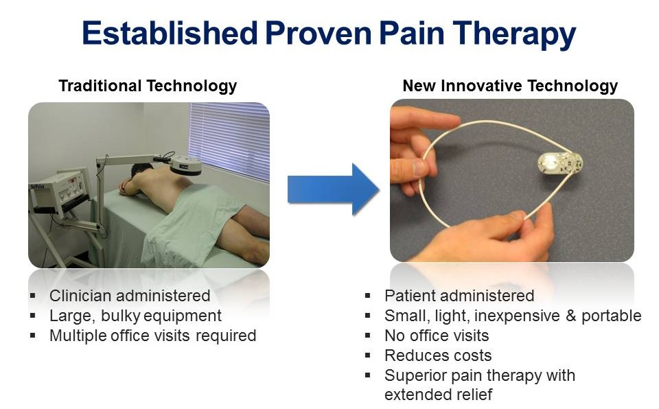
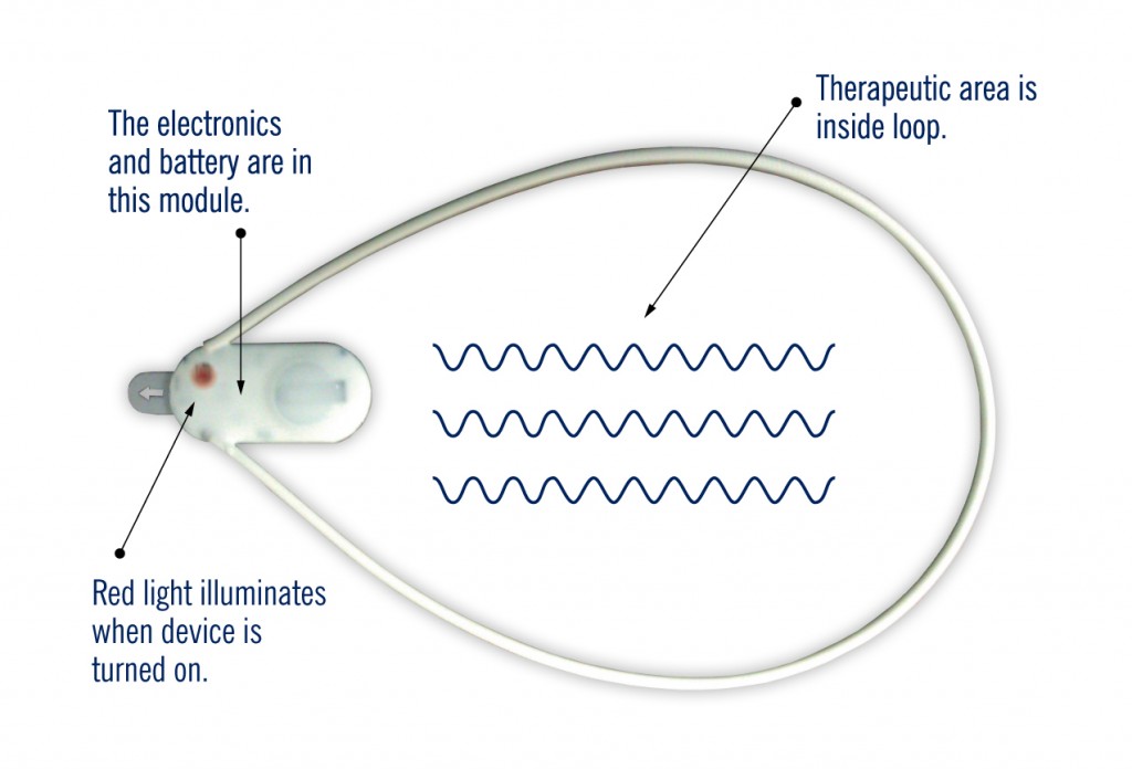
BioElectronics has developed a miniaturized wearable pulsed shortwave diathermy device. The concept is replacing short duration, high power treatments in the clinic delivered by a trained professional, with an easy to use, self-administered, very low power device that can be used 24 hours per day.

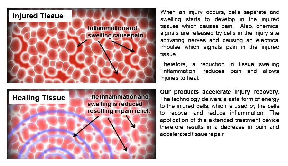
Pain is caused by inflammation, which is a swelling in the tissues of the body that then puts pressure on nerves causing pain. Chemical signals are also released by damaged cells in inflamed tissue that activate the nerves changing a chemical signal into an electrical impulse that causes pain for the body. Inflammation can be both acute, occurring immediately after an injury, or chronic (long lasting) inflammation which is unhealthy and can linger for months or years. Many diseases have been linked to chronic inflammation.
Para mas información: 

ECME 2013

Para información : 
Hay un congreso titulado ECME 2013, el cual habla de electrónica Molecular. Los invito a checar la información: 


It is our great pleasure to welcome you to the 12th European Conference on Molecular Electronics, held in London on 3 – 7 September 2013.

The European Conference on Molecular Electronics, ECME, has become the premier European Conference in the field, and ECME 2013 will belong to the prestigious series of biannual conferences previously organized in Italy (Padua, 1992), Germany (Kloster Banz, 1994), Belgium (Leuven, 1996), Great Britain (Cambridge, 1997), Sweden (Linköping, 1999), The Netherlands (Rolduc, 2001), France (Avignon, 2003), Italy (Bologna, 2005), France (Metz, 2007), Denmark (Copenhagen 2009) and Spain (Barcelona, 2011). ECME 2013 will take place at Imperial College’s Great Hall from September 3 – 7, 2013.

The conference will cover all areas related to organic electronics and photonics, including chemistry, physics, biology, materials science, nanoscience, device engineering and commercialisation, with sessions on the following themes:
- Interfaces
- Bioelectronics
- Light Harvesting and Energy
- Charge Transport
- Photophysics
- Spintronics
- Single Molecules
- Lighting and Photonics

Eight plenary speakers will present their latest research along with 24 invited speakers. The program will also include 16 invited short talks (predominantly by Early Career Scientists), contributed talks and two poster sessions, held at the London Science Museum’s Flight and Modern World Galleries, Conference dinner will be held in the Main Hall of London’s Natural History Museum.

Los invito a checar la información en el siguiente link: 

Locally Altering the Electronic Properties of Graphene by Nanoscopically Doping It with Rhodamine 6G


We show that Rhodamine 6G (R6G), patterned by dip-pen nanolithography on graphene, can be used to locally n-dope it in a controlled fashion. In addition, we study the transport and assembly properties of R6G on graphene and show that in general the π–π stacking between the aromatic components of R6G and the underlying graphene drives the assembly of these molecules onto the underlying substrate. However, two distinct transport and assembly behaviors, dependent upon the presence or absence of R6G dimers, have been identified. In particular, at high concentrations of R6G on the tip, dimers are transferred to the substrate and form contiguous and stable lines, while at low concentrations, the R6G is transferred as monomers and forms patchy, unstable, and relatively ill-defined features. Finally, Kelvin probe force microscopy experiments show that the local electrostatic potential of the graphene changes as function of modification with R6G; this behavior is consistent with local molecular doping, highlighting a path for controlling the electronic properties of graphene with nanoscale resolution.


Bibliografía:

Nano Lett., 2013, 13 (4), pp 1616–1621
DOI: 10.1021/nl400043q
Publication Date (Web): March 13, 2013
Copyright © 2013 American Chemical Society

Hot exciton dissociation in polymer solar cells


The standard picture of photovoltaic conversion in all-organic bulk heterojunction solar cells predicts that the initial excitation dissociates at the donor/acceptor interface after thermalization. Accordingly, on above-gap excitation, the excess photon energy is quickly lost by internal dissipation. Here we directly target the interfacial physics of an efficient low-bandgap polymer/PC60BM system. Exciton splitting occurs within the first 50 fs, creating both interfacial charge transfer states (CTSs) and polaron species. On high-energy excitation, higher-lying singlet states convert into hot interfacial CTSs that effectively contribute to free-polaron generation. We rationalize these findings in terms of a higher degree of delocalization of the hot CTSs with respect to the relaxed ones, which enhances the probability of charge dissociation in the first 200 fs. Thus, the hot CTS dissociation produces an overall increase in the charge generation yield.


Grancini, Maiuri, Fazzi, Petrozza, Egelhaaf, Brida, & Cerullo. (09 de 12 de 2012). Hot exciton dissociation in polymer solar cells. Nature Materials, 29-33.


viernes, 17 de mayo de 2013

SiLEDs

Los científicos de KIT y la Universidad de Toronto / Canadá han tenido éxito en la fabricación de diodos emisores de luz basados ​​en silicio (SiLEDs). Ellos son libres de metales pesados ​​y pueden emitir luz en varios colores. El equipo de químicos, materiales de investigadores, nanocientíficos y expertos optoelectrónicos presenta su desarrollo en el Journal Letters Nano.

la fabricación de silicio de diodos emisores de luz se ha limitado a la gama espectral visible de color rojo y el infrarrojo cercano. En cuanto a la eficiencia de los diodos de silicio que emiten luz roja, los investigadores de Karlsruhe ya son de primera en el mundo. . Científicos KIT ajustataron  específicamente el color de la luz emitida por los diodos por la separación de las nanopartículas en función de su tamaño.  Los diodos emisores de luz tienen una  estabilidad a largo plazo que no se ha llegado antes,e l aumento de la vida útil de los componentes en funcionamiento es debido a la utilización de nanopartículas de un tamaño solamente. Esto mejora la estabilidad de los componentes de película delgada sensibles. Se excluyen cortocircuitos debido a las partículas de gran tamaño.

Los SiLEDs también tienen la ventaja de que no contienen metales pesados. A diferencia de seleniuro de cadmio, sulfuro de cadmio o sulfuro de plomo utilizado por otros grupos de investigadores, el silicio utilizado por este grupo para las nanopartículas de emisión de luz que no es tóxico. Por otra parte, está disponible a bajo costo y altamente abundante en la tierra. Debido a sus muchas ventajas, los SiLEDs se seguirán desarrollando en cooperación con otros socios.

Más información: http://phys.org/news/2013-02-silicon-nanocrystal.html  

World's smallest semiconductor

Se ha creado un laser semiconductor en la universidad de Texas con la ayuda de Taiwan y China, este laser esta construido por un nanorod de nitruro de galio con indio, ambos usados en LED, el nanorod es localizado en una delgada capa de silicon. El campo electromagnético resonante se concentra en la capa de dióxido de silicio en una brecha de 5 nm de espesor insertado por el  nanorod y la película de plata atómicamente lisa.
Los nanolasers, son dispositivos fotónicos podrían utilizar nanolásers para generar señales ópticas y transmitir información, y tienen el potencial para reemplazar los circuitos electrónicos. Sin embargo, el tamaño y el rendimiento de los dispositivos fotónicos se han limitado por lo que se conoce como el límite de difracción óptica tridimensional. 
Los nanoláseres como éste podrían permitir el desarrollo de chips que todos los procesos están contenidos en el chip, los llamados sistemas de comunicación "on-chip". Esto evitaría que las ganancias de calor y la pérdida de la información típicamente asociada con dispositivos electrónicos que pasan los datos entre varios chips.

más informacion:  http://www.utexas.edu/news/2012/07/26/smallest-semiconductor-laser-created-ut-scientists/

jueves, 16 de mayo de 2013

Electrically conductive yarns have attracted consider- able attention because of their desirable properties including electrical conductivity, flexibility, electrostatic discharge, electromagnetic interference protection and radio frequency interference protection. The development of conductive yarns is also critical for various applications in wearable electronics such as wearable displays, solar cells, actuators, data managing devices, and biomedical sensors. Conductive yarns directly spun from conductive materials including metals, metal oxides, carbon nanotubes (CNTs), and conducting polymers were first demonstrated as prototype materials for wearable electronics, yet they are expensive and difficult to be produced on a large scale A more economic and productive way of making conductive yarns is coating conventional fibers with a layer of metals, CNTs, or conducting polymers, followed by spinning into yarns. Cotton, cellulose in nature, is the most widely used natural fiber in the world. It is low-cost and clean to produce, and has a wide variety of applications in textile clothe, upholstery, daily care, and medicine To address the challenge, this group of scientist reported a novel, facile, and versatile approach for preparing highly durable, electrically conductive cotton yarns by electroless deposition (ELD) of metal particles onto cotton yarns modified with polyelectrolyte brushes as adhesion layer. The process is really interesting, and can be seen in the following figure. The resulting yarns were tested as wires to power LEDs, it can be seen that they don’t need more cables or conducting glue, just a DC power (battery) and put the LED into the fabric. It turns on as it was connected with normal wires. This yarn can help to produce electronic textiles because of its great conductive properties.


Xuqing Liu, Haixin Chang
Electrically conductive yarns have attracted consider- able attention because of their desirable properties including electrical conductivity, flexibility, electrostatic discharge, electromagnetic interference protection and radio frequency interference protection.
The development of conductive yarns is also critical for various applications in wearable electronics such as wearable displays, solar cells, actuators, data managing devices, and biomedical sensors.
Conductive yarns directly spun from conductive materials including metals, metal oxides, carbon nanotubes (CNTs), and conducting polymers were first demonstrated as prototype materials for wearable electronics, yet they are expensive and difficult to be produced on a large scale
A more economic and productive way of making conductive yarns is coating conventional fibers with a layer of metals, CNTs, or conducting polymers, followed by spinning into yarns.
Cotton, cellulose in nature, is the most widely used natural fiber in the world. It is low-cost and clean to produce, and has a wide variety of applications in textile clothe, upholstery, daily care, and medicine
To address the challenge, this group of scientist reported a novel, facile, and versatile approach for preparing highly durable, electrically conductive cotton yarns by electroless deposition (ELD) of metal particles onto cotton yarns modified with polyelectrolyte brushes as adhesion layer. The process is really interesting, and can be seen in the following figure.

The resulting yarns were tested as wires to power LEDs, it can be seen that they don’t need more cables or conducting glue, just a DC power (battery) and put the LED into the fabric. It turns on as it was connected with normal wires.
This yarn can help to produce electronic textiles because of its great conductive properties. 

Toward All-Carbon Electronics: Fabrication of Graphene-Based Flexible Electronic Circuits and Memory Cards Using Maskless Laser Direct Writing


Jiajie Liang, Yongsheng Chen 

Graphene is emerging as a novel 2D material in the field of materials science because of its intrinsic electronic, thermal, mechanical, structural and chemical properties. How ever, to fully realize its potential for all the proposed devices, once key is to develop an easy method to fabricate patterned graphene films.
Lately, the advanced technique of laser direct cutting, which has the advantages of maskless, rapid prototyping, reliability, amenability, upward scalability, and low cost, is of increasing importance in device fabrication and has been used to construct microstructures on various films of semiconductor, metal, and dielectric polymer
However, it is still a big step away using this technique to meet the need for fabricating the real-world micro/nano- electronic circuits and devices. To date, two key issues remain for this technique. First, the silicon-based semiconducting microstructures fabricated with the laser-writing technique make it rather difficult to have a clean structure and thus are unusable because of the nonvolatile remains. Second, as to the fabrication of organic or polymer films using this technique, their relatively poor chemical stability and resistance likewise extremely handicap their further use in this field. In this paper, the researchers describe a maskless process to fabricate all-carbon electronic circuits using a continuous graphene film prepared from a graphene solution spin-coating process followed by maskless laser writing.
Of great significance is that this writing process could be operated directly in air at ambient conditions, and various patterns used for electrical circuits and devices can be easily achieved.
On this basis, a novel prototype of write-once-read-many-times (WORM) memory cards along with a data-retrieving system has been demonstrated, the WORM were made on different substrates: flexible polyimide, quartz, and glass substrates. Then and graphene oxide solutions were spin coated to get uniform thin layers. Finally they were reduced to have graphene, over them small thin-film gold squares were deposited to act as the electrodes.

Remarkably, owing to the extraordinary chemical stability of graphene, these graphene-based WORM memory cards possess almost infinite data retention time and extreme reliability, which are crucial in the practical use of some memory devices, such as identification cards, radio- frequency tags, passports, e-tickets, and military applications.

“Double Exposure Method”: a Novel Photolithographic Process to Fabricate Flexible Organic Field-Effect Transistors and Circuits


Organic electronic devices are the expectation of future electronics due to its great potential mainly flexible electronics. But there are some limitations in the development of practical applications. It’s urgent to develop effective high-resolution patterning techniques. Photolithography show overwhelming advantages in reducing the minimal feature dimensions over other conventional printing techniques, with which high resolution highly integrated organic transistors could be fabricated.
Before getting into fully organic electronic devices there is the promise of making hybrid systems that have both Si electronic components and organic components. One of the applications of organic polymers that has been studied is to use them as dielectric material, replacing SiO2 in conventional transistors. How ever, the use of organic polymers has the problem that many of them cannot endure conventional photolithography.
To solve these problems the researchers developed a novel photolithographic method called “double exposure method”. They starter with a Polysterine thin film spin coated over ITO/PET and annealed at 80º C. Then a photoresist was spin coated over the PS film and UV irradiated, patterned for the electrodes and irradiated again. Then a thin gold film was deposited and washed with a solvent and exposed again to the method. And finally deposited organic semiconductors of 50 nm (pentacene). This process was also used for other logic circuits.

Characteristic curves showing the performance of the OFET


In summary, they developed and tested a method to fabricate flexible organic field effect transistors and circuits. The performance obtained  was comparable to the ones from traditional Si techniques.