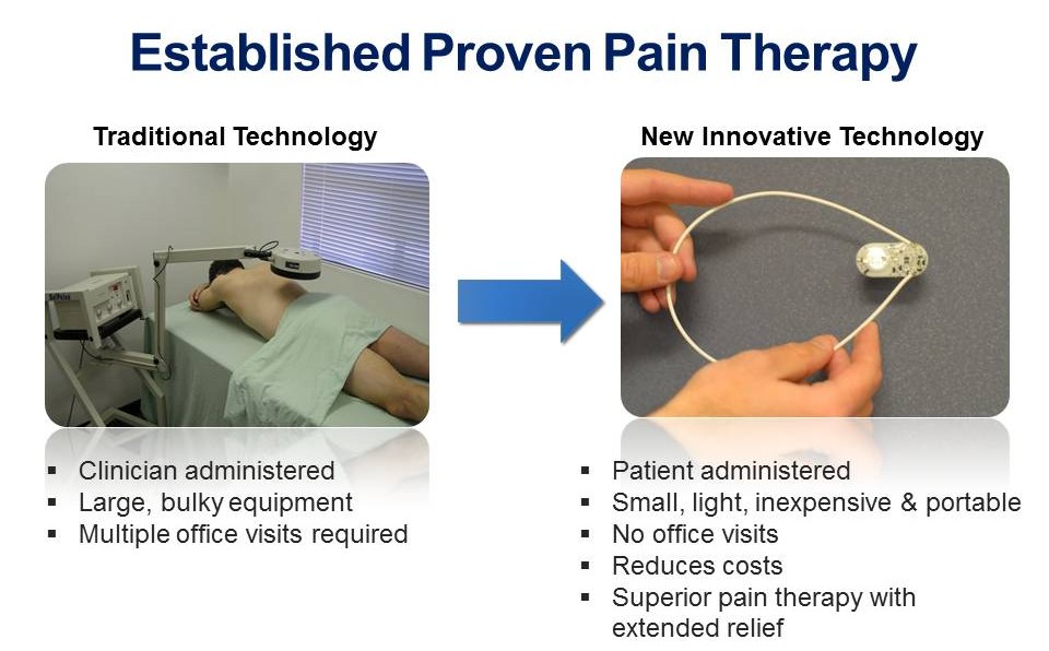
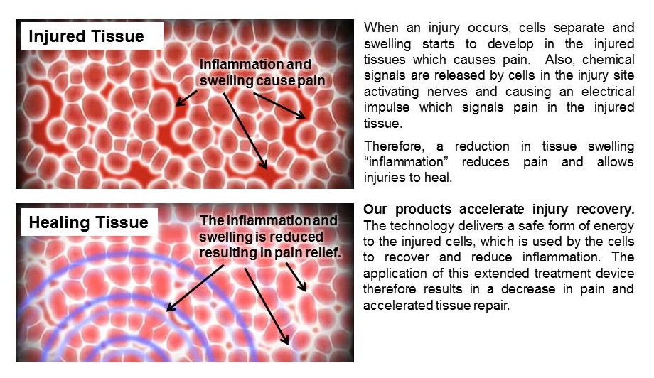
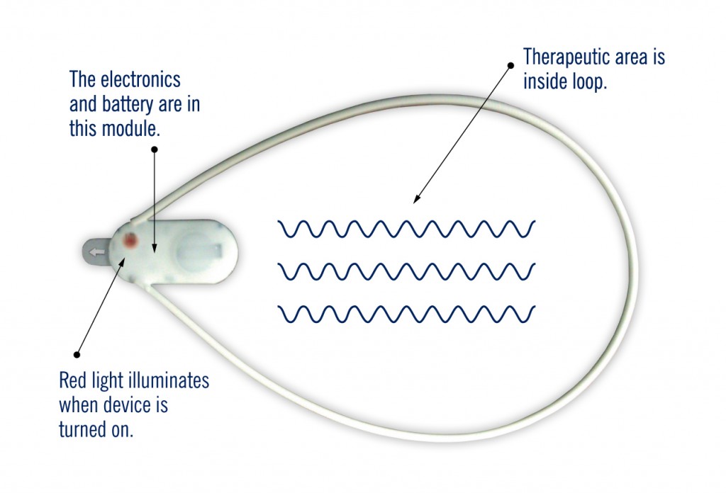
WIRED
The Next Big Thing is very, very small. Picture trillions of
transistors, processors so fast their speed is measured in terahertz, infinite
capacity, zero cost. It's the dawn of a new technological revolution - and the
death of silicon. Can you say Thiophene Ethynylene Valley?
By Rick Overton
Once again, Jim
Tour has forgotten to breathe.
Sitting in his
office at Rice University in Houston, he's telling the story of how he was
heckled while giving a speech at the 1995 Marvel Symposium in Tucson, Arizona -
an event that attracts the world's foremost chemists - and it's making him even
more animated than usual. In the throes of his reenactment, it seems he might
forgo even the most basic involuntary function.
"One guy,
one guy, head of a big institute in Europe, sat there, sat there while I was
speaking, and he went like this ..." Tour crosses his arms, curls his face
into a dour expression, and shakes his head.
Tour had spent
hours at the conference listening to his colleagues recount their journeys
along well-worn research paths toward cheaper pharmaceuticals, stronger
plastics, and so on. During his own presentation, however, he revealed plans
for an upcoming experiment so unusual that few in the crowd took him seriously.
His experiment,
he told the audience, would measure current flowing through an individual
molecule. At the time, this was a daring proposition, since the ability to
manipulate - even to see - matter at that scale was brand-new.
"You can't
do that!" the heckler bellowed. "You can't isolate a single
molecule like that, and I will give reasons why in my talk."
Tour, an unimposing
man with short black hair and an easy smile, relishes telling the story. He's
hamming it up, with arms crossed, neck puffed out, head nodding arrogantly. He
looks like an Italian comic imitating Il Duce.
"The
molecules are moving too rapidly on the surface!" another scientist chimed
in. Tour plays him with a mild Tourette's shake, spitting sentence fragments.
"You'll never be able to isolate just one of them!"
Again Tour's
voice begins to falter for want of air. He stops, breathes, leans toward me,
and says softly, "I told him we were three months from trying this
experiment. Three months away. 'Should I not even try?' I asked him.
'Should I stop right here?'"
Long pause.
"I knew I
had him," Tour says. "No scientist would ever say, 'Based on what I
say, you shouldn't even try it.'
"Well, I
tried the experiment, and you know what? It worked."
Tour's
specialty is inventing molecules with novel attributes, but it's up to his
research partner, a soft-spoken electrical engineer named Mark Reed, to test
them. In a basement at Yale, Reed measures their conductivity and other
electrical properties using a Frankenstein's lab of arcane machinery, such as a
scanning tunneling microscope with a "lens" that consists of a single
atom.
For 10 years,
Tour and Reed have been nurturing the nascent science of molecular electronics,
or moletronics. In the last year and a half, they have progressed well beyond
the basic principle Tour suggested at the Marvel Symposium. His newest
molecules exhibit semiconductive properties that give them the ability to hold
a charge or behave like switches or memory, meaning molecular electronics could
replace the transistors, diodes, and conductors of conventional microelectronic
circuitry. If Tour and Reed's experiments continue to advance at a steady pace,
within a decade moletronics will be able to do nearly everything currently done
using silicon - and more.
Molecular
microchips, populated with transistors that can be produced cheaply in
astronomical numbers, will compute faster, remember longer without needing to
be refreshed, and consume power at a mere trickle. More immediately,
moletronics will transcend the limitations of magnetic and optical storage
technologies, providing memory systems so powerful, small, and inexpensive that
the entire Internet could be cached on a single desktop. Or, as Tour's
associate Thomas Mallouk puts it, "Imagine a computer that remembers every
keystroke you've ever made, with more storage capacity than you could ever
need."
These possibilities have sparked an excitement that
harks back to the invention of the silicon chip. R&D dollars are being
lavished upon moletronics labs at IBM, Hewlett-Packard, and the Mitre
Corporation, which are scrambling to convert theory into technology and produce
the first commercial molecular chips and memory systems.
Some of this money has found its way into a
brand-new company, Molecular Electronics Corporation, founded in late 1999 by
Tour, Reed, and several colleagues in an effort to ride the tide their science
is setting in motion. When it recedes, the world will be a very different
place.
Chemistry was not Jim Tour's first love. "I
was going to be a New York state trooper," says the 40-year-old from White
Plains. "I really had this thing about law enforcement and driving a big
Chrysler up and down the highway, but I couldn't get into the academy because I
was colorblind." So instead Tour got an undergraduate degree in chemistry
from Syracuse University in 1981 and earned his PhD at Purdue five years later.
After two one-year postdocs at Wisconsin and Stanford, he went to the
University of South Carolina in 1988 to teach chemistry and do research.
Reed, 45, grew up in Syracuse and received both his
BS and his PhD in physics from Syracuse University. In the 1980s, he made a
reputation at Texas Instruments through his work on quantum dots (minute
droplets of semiconductor material). In 1990, he took a respectable academic
post at Yale and set out to find a leading-edge field that posed more questions
than answers.
Tour and Reed are a bit of an odd couple. Tour is a
natural stage presence, a man of faith who not only was denied a career in law
enforcement but resisted an instinct for missionary work. Reed is genial,
casual. He tends toward scientific conferences located near scuba-diving hot
spots.
Although the
two had met as students at Syracuse, they first discovered they had a common
interest at a small gathering of moletronics researchers in the Virgin Islands
in December 1991. The meeting was hosted by Ari Aviram, one of the field's
founding fathers, who now works at IBM's Thomas J. Watson Research Center in
New York. In 1975, he and theoretical chemist Mark Ratner, then at New York
University and now at Northwestern, published a paper in Chemical Physics
Letters proposing that individual molecules might exhibit the behavior of
basic electronic devices. Their hypothesis, formulated long before the means
existed to test it, was so radical that it wasn't pursued or even widely
understood for another 15 years.
At the Virgin
Islands conference, Tour gave a lecture on how to synthesize some of the
molecules that Aviram and Ratner had envisioned. Reed happened to be sitting in
on the session, and when he heard Tour's talk he realized he had found a
kindred spirit.
"A few days after the meeting," Tour
recalls, "Mark called me and proposed that we submit a white paper to
Darpa." Tour agreed, and Reed drafted a proposal asking for about $1.5
million. The Defense Advanced Research Projects Agency, of course, is in the
business of backing precisely this kind of risk-taking research, and in 1992
the agency funded Tour and Reed for an initial period of three years. Despite
Reed's humble appraisal of the first five years as a time of nearly total
failure, spent "stumbling over every tree stump in the forest," Darpa
has renewed its support every three years, each time with a taller pile of
money.
Silicon technology will reach fundamental limits by 2017. The party
driven by Moore's law will be over.
Today, in a
network of labs spread across two floors at Rice's Center for Nanoscale Science
and Technology, Tour, along with his colleagues and students, spends his time
designing novel molecules. Phenylene ethynylene, for instance, acts as a kind
of wire that transmits electrons. Thiophene ethynylene is a carbon-sulfur
hybrid that shows promise as a semiconductor.
Tour builds
large and small compounds, sometimes assembling a chain of homogeneous atoms,
sometimes fashioning a twisted necklace of strings and loops. Like a jazz
musician, he manipulates the materials of his craft - the nature of the bonds,
the number and position of atoms, the chemical groupings - and with each new
riff produces a different variation.
When Tour finds
something interesting, he ships vials of the material to New Haven, where Reed
and his Yale graduate students cart them down into their basement lab for the
next step. Although they have managed to address individual molecules via a
laborious process that involves bending a wire until it breaks and trapping a
single molecule between the broken ends, molecular wiring remains a major
technical hurdle. (The circuitry in a silicon microchip is made up mostly of
interconnects, and there's little reason to think that molecular chips will be
any different.) For now, Reed works on groups of roughly 1,000 molecules - still
1,000 times smaller than the smallest silicon transistor.
It was in the subterranean stillness of Reed's lab,
around Thanksgiving 1998, that the pair made one of the most dramatic
breakthroughs in molecular electronics to date. Tour had synthesized a molecule
with the unwieldy name
2'-amino-4,4'-di(ethynylphenyl)-5'-nitro-1-benzenethiolate - or ethynylphenyl
for short. Reed's star graduate student Jia Chen poured a solution containing
ethynylphenyl molecules onto a nonconductive substrate of silicon nitride and
silicon oxide pocked with nanopores - holes 30 nanometers in diameter - with
gold at the bottom. Like glitter sprinkled over glue, the molecules adhered to
the gold surface, spreading out into a single layer. Chen evaporated a
conductive layer of gold on top of the ethynylphenyl molecules and bonded the
sandwich to a socket. Then she wired the assembly to a semiconductor parameter
analyzer, a device capable of detecting even the slightest flow of electricity.
"Suddenly I saw a rise and fall in the
current," Chen recalls. "At first I thought something was wrong. But
I went back and did it again, and I saw a very sharp switch type of
behavior."
As described in
November 1999 in Science, the experiment demonstrated the first
reversible molecular switch. Tour and Reed had been on the right track all
along, and Aviram and Ratner's hypothesis, now 23 years old, had proven
correct.
"It's why
I do this job," Reed says. "I'm not here to get rich. I'm not here to
minimize my work hours, believe me. I do it for the excitement."
Tour and Reed's experiments might put a lot of chip
engineers out of work, and it might happen soon. According to the captain of
the $143 billion semiconductor industry, Intel cofounder Gordon Moore, silicon
doesn't have much time left.
On September 30, 1997, standing before a roomful of
developers at San Francisco's Moscone Convention Center, Moore showed the
audience an electron micrograph of a Pentium chip on a high-resolution
projector. He called attention to the chip's very thin logic: "As you can
see, it's only several molecular layers thick. I don't know how much more you
can expect to scale that without beginning to see some real problems. So at
some time in the next several generations, we really start to get to some
fundamental limits."
A semiconductor
transistor is essentially a region of crystalline silicon with three terminals
- conductive paths into and out of the crystal - called gate, source, and
drain. If a voltage is applied to the gate terminal, current can flow from the
source through the crystal and out the drain. Turn off the gate voltage and
current can't flow. The role of a transistor is to control this binary
switching between on and off - the 1 and 0 of digital electronics. The
professional lives of chip engineers are devoted to packing more and more
switches onto wafers of silicon, despite stubborn physical limits and
ridiculously short product life cycles. The more switches per wafer, the faster
the resulting chip's performance.
Chip
performance had been increasing predictably for generations when Moore warned
his audience about silicon's fate. "We can expect to see the performance
of our processors double every 18 to 24 months for at least several
years," he began, summarizing what is known as Moore's law. But packing
more and more devices onto a chip means etching smaller and smaller patterns
into silicon, which requires increasingly precise equipment and more
challenging quality control - all of which adds up to ever higher costs.
"If you extrapolate ... we run out of gas doing that in the year
2017," Moore concluded. "That's well beyond my shift."
This
phenomenon, the effects of which are only beginning to be felt, might be called
Moore's second law: As engineers approach the physical limits of scale, the
cost of fabricating chips will increase exponentially and eventually overtake
the savings generated by the first law.
A new fab plant
already costs upward of $1.5 billion. If Moore is right, the next generation
could cost $3 billion, and each succeeding wave of plants would double in
price. Two aspects of the chip economy that have been taken for granted for 30
years - falling prices and increasing speeds - will fade, and finally, 15 or 20
years from now, disappear. In the world of silicon, the party will be over.
"With moletronics you build your transistors in a pot, a year's
supply at a time." The key: self-assembly.
Tour and Reed
were acutely aware of Moore's prophecy when Chen fired the first electrical
charge through that ethynylphenyl-coated wafer, and they're counting on
moletronics to pick up the slack.
"Eighteen
milliliters of water - one swallow - contain six times 1023 molecules,"
Tour says, pausing for a moment to allow the number to sink in. "If you
could stack up that many sheets of paper, they would reach the sun 400 million
times. I can make that many molecules in a flask in three days."
Millions of
transistors are etched on the face of a Pentium chip. But when millions of molecular
devices take up the space occupied by one transistor, the sheer computing power
will be millions of times that of silicon, revolutionizing current notions of
processor speed.
Another major
advantage of molecular devices involves the manufacturing process. To make a
microchip, you have to etch a complex pattern of millions of transistors and
interconnects onto the surface of a silicon wafer. "That involves about 28
or 30 lithographic steps," says IBM's Aviram. Moletronics can eliminate most
of these steps and compress the schedule into a matter of hours, thanks to a
chemical phenomenon known as self-assembly. Instead of trying to build chips
one component at a time, chemists might simply put the right ingredients in a
beaker, apply very specific conditions, and watch the molecules assemble
themselves in proper order on a substrate. In this regard, the manufacture of
molecular electronics is closer to pharmaceutical production than the
chipmaking process.
The cost
savings will be hard to estimate until a molecular production facility is in
operation, but they are expected to be tremendous. "With molecular
electronics," Aviram says, "you build your transistors in a pot, a
year's supply at a time."
"You are
only dipping things in chemical baths, so you can print, build, or glue
molecules onto just about any substrate - plastic, wallpaper, it doesn't really
matter," notes Brosl Hasslacher, a staff theoretical physicist for the
Complex Systems Group at Los Alamos National Laboratory. "The result is an
incredible amount of information capacity at almost zero cost."
Semiconductor technology was patented in 1928, long
before anyone really knew what to do with it. It wasn't until 1947 that the
first crystal transistor was invented at Bell Labs. "The time it took from
the first transistor to the demonstration of an integrated circuit was 11
years. We've just built the first molecular transistor," Reed says with a
smirk, "so now we've got 11 years."
That's more
glib than true, and he knows it. Researchers in moletronics initially thought
they were in for 10 to 15 years of occasional successes and incremental
progress. But new infusions of support and a spate of breakthroughs suddenly
have everyone counting the months, rather than years, until a product hits the
market.
Bill Clinton mentioned molecular computing in his
final State of the Union address and proposed that nearly half a billion
dollars be directed to nanotechnology research in 2001. The biggest magnet for
those R&D dollars is the group of 10 primary moletronics projects currently
funded by Darpa at Harvard, Hewlett-Packard, the Mitre Corporation, Notre Dame,
Penn State, Rice, UC Riverside, University of Colorado, UCLA, and Vanderbilt.
(Reed, at Yale, is collaborating with researchers at Harvard, Penn State, and
Rice.)
All these projects are trying to bring the first
molecular computing product to market, but with a 10-year head start, Tour and
Reed are confident that they can win the race. In November, with an undisclosed
pile of cash, they cofounded Molecular Electronics Corporation (MEC), leasing
lab space in New Haven and in the Nittany Valley near Penn State.
Tour and Reed
recruited two chemists from Penn State - Thomas Mallouk, professor of
chemistry, and David Allara, professor of materials science and chemistry. Both
have made breakthroughs in molecular-scale wiring that will be key in
assembling a device. Hasslacher rounds out the technical team with his deep
understanding of molecular devices and system architecture. All five scientists
have joined the company as directors, but for now they remain occupied
primarily by their academic and research posts.
To run the business end of the company, the group
brought in Harvey Plotnick, a philanthropist and trustee of the University of
Chicago. Plotnick's tech credentials are thin: He owns Einstein's handwritten
notes on the general theory of relativity, but he made his money in publishing.
Nonetheless, when he met the five scientists and a handful of early investors
in Santa Fe in January, each party thought the other a good fit.
Plotnick, whose salary is $1 a year, is shy about
naming early investors. "We have enough cash in our account today to get
through two years," he says. "And I have firm offers of equity money
to get beyond that, should we need more."
Already the upstart company has a deep-pocketed
rival. In the mid-'90s, when big corporations were scaling back basic research
to develop fast-track technologies, Hewlett-Packard bucked the trend, forming a
research team in Palo Alto. R. Stanley Williams signed on as lead scientist.
Stan Williams says he was "a dumb hick from
South Texas" until he arrived at Rice University in the early '70s. He
quickly fell under the tutelage of chemist Robert Curl, who would go on to
share a Nobel Prize in 1996 with Sir Harold Kroto of the University of Sussex
and Richard Smalley, another Rice chemist, for their discovery of a class of
carbon molecules known as fullerenes. After earning a PhD at Berkeley, Williams
spent 2 years at Bell Labs and 15 years at UCLA before he came to the rolling
hills of Palo Alto in 1995 to do head-scratching science for HP.
Williams was familiar with Tour and Reed's research
but doubtful about its potential until he saw the work of one of his own HP
scientists, Phil Kuekes, who had designed a new type of defect-tolerant
computer architecture. Kuekes, a veteran builder of massively parallel systems
for use in radar installations and weather modeling, had engineered a
fridge-sized experimental machine called the Teramac. The Teramac weighed 400
pounds and had 220,000 known defects. Even a single hardware defect can bring
down a conventional computer system, but Kuekes engineered a redundant
architecture capable of learning to skirt around its own errors.
Williams knew that a computer system built around
molecular devices would need to be smarter than silicon about naturally
occurring defects, and he saw the Teramac as a prototype for this kind of
computer.
"They call moletronics a disruptive technology," Hasslacher
says. "I don't. I call it a predator."
As Tour and
Reed are quick to acknowledge, every transistor on a silicon wafer can be
tested individually, because each is connected to unique input and output lines.
Molecular researchers still need to either figure out a way to address millions
of densely packed molecules individually or devise a system that can deal with
disorder and impurities. Kuekes' architecture appeared to address this
fundamental problem.
In 1996, Hewlett-Packard formalized its moletronics
research in a partnership with UCLA that appears to compete directly with Tour
and Reed's MEC. HP recruited Fraser Stoddart and Jim Heath, two UCLA chemists
who have spent many years searching for the elusive bridge between chemistry
and electrical engineering.
Stoddart, a
Scot who speaks in a thick brogue, started his career in what he calls
"the hierarchical nonsense" of British academic institutions, and
he's pretty happy these days to be in the free-for-all world of science
American-style. At UCLA, he synthesized a molecule called rotaxane, which
looked like a sliding counter on an abacus rod. Rotaxane turned out to be a
non-reversible switch (flip it on once and that's all she wrote), and it became
the basis for designing molecular logic gates and read-only memory.
Heath is a
seasoned chemist who, as a graduate student at Rice, assisted Smalley with his
fullerene experiments and worked with Kuekes on adapting the Teramac for
moletronics. Today, like Stoddart, he oversees a group of graduate students
doing research on metal and semiconductor nanocrystal structures.
So what can we expect the two competitors - HP and
MEC - to bring to market? Most observers agree that the first commercial
application will be molecular memory. Tour has constructed molecules that capture information by trapping
electrons in a region called the lowest unoccupied molecular orbital (LUMO). A
molecule whose LUMO has no electrons doesn't conduct current and represents a
bit value of 0. Having trapped one electron, the molecule becomes conductive,
representing a 1. When it traps a second electron, the LUMO is filled and
current can't flow, so the value reverts back to 0. The whole cycle takes less
than a trillionth of a second, "which is at least three orders of
magnitude faster than computers are right now," Tour says. Moreover,
current LUMO designs can hold a bit for 10 minutes without further need for
electricity - in contrast to silicon DRAM's milliseconds.
Just how the research teams plan to turn this
simple electrochemical reaction into a memory system capable of storing almost
unlimited amounts of data is a well-guarded secret - at least for now.
Universities and corporations are negotiating key patents behind closed doors.
Dramatic new research results are queued up for publication in various
scientific journals, which keep all new studies strictly under wraps. As
moletronics is readied for the mainstream, it seems, everyone is keeping mum.
"These aren't trade secrets," Williams
allows. "All of this stuff is going to get published just as soon as
possible. But there's just a lot we can't discuss right now."
Tour is similarly evasive. "There's certain
work that we do for Darpa that we can be open about," he explains,
"but with MEC there's a ton of money at stake."
Industry
observers from Intel to the White House are watching and waiting to see how
moletronics might shake up the entrenched silicon empire. And given what we now
know about the chip industry - the fragility of market share, the pace of
change, the rising cost of manufacturing - you'd think there would be some
antipathy toward this upstart field. But the silicon industry hasn't yet taken
much notice.
"I don't get the sense that there's a terrible
panic in the semiconductor industry," says Rick Smalley, whose office is
in the building next to Tour's lab. When I drop by to see him, I notice a giant
plastic buckyball - a fullerene that self-assembles 60 carbon atoms into the
shape of a soccer ball - sitting on his couch. An eminent scientist who
frequently advises presidents and members of Congress, Smalley believes that
molecular electronics is likely to sneak up on the solid-state crowd.
"You might just wake up one day and see, in
the morning's New York Times, some group of kids someplace has come up
with a memory that's got a terabyte of capacity and costs less than 10
cents," he says. "And you can weave it into your shirt."
When Smalley
and his fellow researchers started lecturing about fullerenes, they too
encountered resistance. But there's nothing like a Nobel Prize to silence
critics. This must be of some comfort to Tour, who has been touting the
electronic properties of molecules for 10 years and will surely have to
tolerate more razzing before he's fully vindicated.
"Are there
individuals who are greatly opposed to moletronics? Yes, and I'd rather not
name them," Tour tells me, waving a finger in the air and laughing.
"They know who they are."
Reed recalls an
Intel engineer who contacted him after articles on moletronics first started
appearing in science journals. Although Reed thought the inquiry was in
earnest, it soon became apparent that the man was fishing.
"He said, 'I have arguments about this, this,
this, this, and this,'" Reed remembers. "He was trying to justify
himself to Intel's internal management by arguing that what we're doing
wouldn't work. It's obviously a different culture."
"These things are small enough to stir into paint; why not embed
countless black boxes in the skin of a plane?"
"A lot of
conservative chemists give people like me a rough time," Stoddart says.
"But isn't this always the case when something new is created? You get
enormous opposition from the bulk of people who aren't comfortable with change.
"For
me," he continues, "the exciting thing about this revolution is that
it's taking scientists out of their boxes. Some of the worst offenders are the
chemists. They've buried their heads in the sand for a century and a half with
labels that say they are this or that particular type of chemist. It has taken
the last quarter of a century to start to break down these barriers within our
own community."
According to
Dan Hutcheson, president of VLSI, a research firm that tracks the microchip
market, "The best way to get engineers to invent new technologies is to
tell them it's impossible. The phenomenon of this industry has been its amazing
ability to solve problems. At places like Rice and Yale, kids working for their
professors are going to create the next industry. For me, molecular electronics
is not a frightening thing. It's an exciting thing."
In 1997's The Innovator's Dilemma, Harvard
business professor Clayton Christensen coined the term "disruptive
technologies" to describe developments capable of displacing and even
bankrupting established market leaders. "They call moletronics a
disruptive technology," Hasslacher says, "but I don't call it that. I
call it a predator. Once you've crossed the threshold with a technology this
cheap and this powerful, it will eat anything else out there in a few years,
changing the whole nature of the game."
In the basement
of Reed's physics building, Yale postdoc Jim Klemic strikes a more conciliatory
note. "Transistors didn't put mechanical switch companies out of business,"
he explains. "There are plenty of switches for high-current applications
that transistors can't handle, like for the voltages and currents that turn on
lamps in a room."
His point is
that it's silly, perhaps even ignorant, to talk about moletronics replacing
silicon in five or ten years. Similarly, Christensen points out that upstarts
usually find a foothold either in low-performance, low-cost areas or by
providing functionality beyond the reach of previous technologies.
Right now,
moletronics researchers are just trying to get the new technology to act like
silicon. They explain moletronics to laypeople by describing it as a
replacement for current computing hardware. But listen more closely and you can
hear a more subtle message. Grown men with million-dollar labs get tongue-tied,
and with gleams in their eyes they tell you they're not exactly sure what these
molecules are capable of. When I press several of them, a stunning future
begins to take shape.
Mallouk foresees an era of hybridization, where
conventional silicon lithography will be used to create templates for
moletronic devices. Imagine, for instance, an nth-generation Pentium ringed by
molecular DRAM.
"These
things are small enough that you could stir them into paint and cover a wall with
them," Kuekes says. "There's a significant software problem in
getting this paint to communicate and self-organize," he adds, but the
possibility isn't far-fetched.
"Airplanes
crash, right? Black boxes, right? Well, why have only one black box?" Klemic
wonders. "Why not embed black boxes throughout the skin of the plane? You
pick up a piece of paint, that's a black box."
"You'll
have enough memory to do augmented reality," Hasslacher predicts.
"We're also coming very quickly to the intersection of molecular systems
and biology, to sensors that interrogate the body. For doctors, this could be
invaluable."
Tour refuses to predict what kinds of devices his
wondrous molecules might bring forth, preferring to stay focused on pure
science. But he brags about chemistry's potential to forever evade Moore's
second law.
"We've got
to stop thinking like the silicon people," he says. "Our chemistry is
too rich. I change just one group on this molecule and boom! The whole
molecular orbital changes and you open up an entirely new type of device. Then
I put a tiny little group onto there, and boom! The whole thing changes again."
With each boom,
more carbon dioxide escapes Tour's body than incoming oxygen can replace. It's
as if he has to expel air to make room for bigger ideas. A minute later he's
breathless again.
"Look," he says, catching up with
himself. "If you get people together who are passionate about something,
you can make anything happen. You just do it."
Spending several days with Jim Tour in Houston, I
begin to see this as his personal slogan: "You just do it." There are
many other factors at work - science, money, research, collaboration, luck -
but it is Tour's sheer force of will, a patent refusal to fail, that will carry
molecular electronics into our lives.
Tour inhales, pauses, then begins again: "You
just push it. This is what we are going to do. We're going to make this happen."
Copyright © 1993-2004 The Condé Nast Publications Inc.
All
rights reserved.
Copyright ©
1994-2003 Wired Digital, Inc. All rights reserved.
 of graphene (Gra) transducers under physiological conditions. We show that suspended Gra devices represent the optimal configuration for cardiac extracellular electrophysiology in terms of both transducer sensitivity, systematically ∼5× higher than substrate-supported devices, and forming tight bioelectronic interfaces. Significantly, noise measurements on freestanding Gra together with theoretical calculations yield a direct relationship between low-frequency 1/f noise and water dipole-induced disorders, which sets fundamental sensitivity limits for Gra devices in physiological media. As a consequence, a square-root-of-area scaling of Gra transducer sensitivity was experimentally revealed to provide a critical design rule for their implementation in bioelectronics